A quantum of coupling
UK startup Zero Point Motion is aiming to disrupt the technology of MEMS sensors with quantum technology.
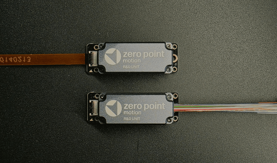
The Bristol-based company is combining lasers and micromachined MEMS structures with quantum sensing in a technique called cavity optomechanics. The company has raised over £6.5m (€7.8m, $8.8m) and is working with two fabs for commercial samples later this year.
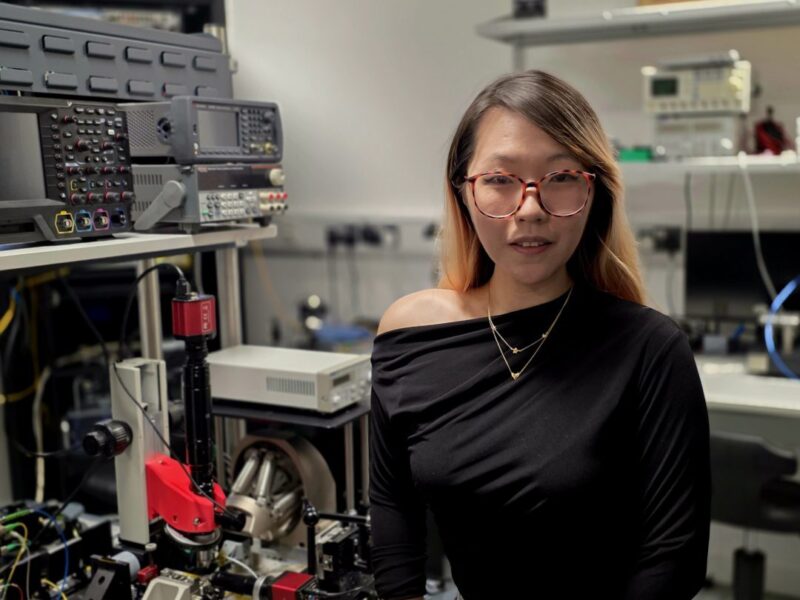
“At the heart of what we do is transforming traditional semiconductor MEMS sensors,” CEO Dr Lia Li (above) tells Nick Flaherty at eeNews Europe. “We have something that can transform the entire semiconductor sensor sector.”
“The key point of cavity optomechanics is to bring a photon as close as possible to a phonon of vibrational energy, it is the quantum of coupling,” she said.
“Then really great things happen where you can couple the phonon to a photon and perform matter interferometry and embed spin states.”
These MEMS sensors have micromachined structures, either as a block or a series of interdigitated fingers, built on standard chip-making process technology. The movement of these masses determines the acceleration for all kinds of applications, from air bag triggers to inertial measurements systems for drones and self-driving cars.
“It is enhancing MEMS with photonics as a fabless startup. That means we get to operate at the true intersection of MEMS and photonics, with design, simulation and testing to shape sensor development going forward.
“One of the challenges is the electrical readout is not so great, that’s why you have so many fingers, so you are limiting your mechanical design space. There’s a lot of coupling to the package and overcrowding with so many capacitor plates and when you make smaller and smaller devices parasitics come into play.”
“My background is all photonics, I’ve built lasers, I understand the power that the laser brings as a tool. I worked at BAE Systems in Filton in the cleanroom building MEMS and interial sensors and its hard to get into that space. That gave me the opportunity for PhD in quantum ground state and cavity optomechanics. It still took many years to connect that to MEMS
Li worked on a business plan when furloughed during the Covid-19 pandemic. This combines a laser waveguide with a ring resonator to measure the movement of the MEMS structure at the quantum level. “At that time I also got to know the University of Southampton and Cornerstone.”
“One of my biggest issues is I’m not a big risk taker,” she said. “I like to back up everything with ten layers of data, so making waveguides by hand was not scalable. As Cornerstone could give us a scalable way to make these, with free tapeouts for waveguides and ring resonators”
The recent announcement by chip giant Nvidia on it’s move into silicon photonics, building ring resonators at foundry TSMC for its chip to chip interconnect, has been significant.
“That’s a big thing for us, it’s a game changer. The more they improve the ring resonator the better it is for us,” said Li.
Unlike Nvidia, though, a startup doesn’t have the resources to customise a foundry process.
“We don’t need to develop a custom flow, we will use the process design kit (PDK). We have patented the cross section of the MEMS on the photonics process but the recipes, they own that, and that’s a fair exchange.
“We have a ring resonator and a waveguide, we then put these at the edge of the mechanical MEMS structure that moves in plane and out of plane on the top surface of the ring. As the gap changes the resonance changes, and we take the readout from the waveguide as the resonance shifts and broadens.”
This approach can use different lasers, a vertical cavity VCSEL or superluminescent SLED, with the ability to tune the sensitivity with different lasers and detectors in the same chip.
This is where the quantum effects come in, with photons entangled with phonons of energy from the vibration of the sensor for extremely accurate measurements.
“You can quantise the motion of the centre of mass and you have a phonon occupancy, and that’s the zero point energy, or the zero point motion,” she said.
Tech transfer
One of the key challenges was the technology transfer from University College London and the technology transfer office.
“You have to fight for fellowships to stay on the track for cavity optomechanics to make sensors and then applied it to business to do the research you want to do, fight for the resources and the freedom to do the research you want to do and that was probably the start of an entrepreneurial mindset.
“Tech transfer was difficult. Traditionally I don’t think technology transfer offices (TTOs) know how to manage physics spin outs. It was rocky and slow, pace was one of the biggest issues. But there are lots of people in the academic system who create really good pathways to work around those bottlenecks.
The recent funding round has opened up the opportunities. Swiss navigation module maker ublox is a key investor and potential customer.
“For us it was network and Gordon [Aspin, founder of Cognovo in Cambridge] as executive chairman, with primarily UK and European investors where there’s a cultural fit, but there’s an Asian investor as well.”
Future
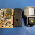
Prototypes are characterised in the laboratory in Bristol, with the packaging technology evolving. She plans to ship engineering samples by the end of 2025 using photonics foundries in the US and Canada. “We see what’s required for quantum technologies to be realised. In solving the problems of the supply chain, moving fast and solving problems, we have inadvertently created a platform technology. That’s IPO material and I want to hold onto that inspiration as long as I can.”
 If you enjoyed this article, you will like the following ones: don't miss them by subscribing to :