Synopsys, TSMC look to 1.6nm backside routing for trillion transistor AI and multi-die chips
Synopsys has disclosed 1.6nm projects for backside power routing that will be key for trillion transistor chips.
Synopsys and TSMC are working on backside routing capabilities supporting TSMC’s A16 1.6nm process in the Synopsys digital design flow to address power distribution and signal routing for its trillion transistor designs that eeNews Europe highlighted back in March.
Interoperable process design kits (iPDKs) and Synopsys IC Validator physical verification runsets are available for design teams to handle the increasing complexity of physical verification rules and efficiently transition designs to TSMC N2 2nm technology. Power is a key factor for these trillion transistor multichip designs.
Mediatek is also developing 2nm chips at TSMC using production-ready AI-driven EDA flows, and a joint TSMC, Synopsys and Ansys multi-physics flow supporting CoWoS interposer packaging addresses thermal and power integrity challenges.
Synopsys looks to AI, 3D die for trillion transistor designs
“TSMC is excited to collaborate with Synopsys to develop pioneering EDA and IP solutions tailored for the rigorous compute demands of AI designs on TSMC advanced process and 3DFabric technologies,” said Dan Kochpatcharin, head of the Ecosystem and Alliance Management Division at TSMC. “The results of our latest collaboration across Synopsys’ AI-driven EDA suite and silicon-proven IP have helped our mutual customers significantly enhance their productivity and deliver remarkable performance, power, and area results for advanced AI chip designs.
“For decades, Synopsys has closely collaborated with TSMC, providing mission-critical EDA and IP solutions spanning all generations of TSMC’s most advanced nodes,” said Sanjay Bali, senior vice president of EDA product management at Synopsys. “This partnership has been instrumental in helping our mutual customers accelerate their innovation in the AI era and advance the future of semiconductor designs. Together, we are pushing the boundaries of what’s possible, enabling groundbreaking advancements in performance, power efficiency, and engineering productivity.”
“Synopsys’ certified Custom Compiler and PrimeSim solutions provide the performance and productivity gains that enable our designers to meet the silicon demands of high-performance analogue design on the TSMC N2 process,” said Ching San Wu, Corporate VP at MediaTek. “Expanding our collaboration with Synopsys makes it possible for us to leverage the full potential of their AI-driven flow to accelerate our design migration and optimization efforts, improving the process required for delivering our industry-leading SoCs to multiple verticals.”
To further accelerate chip design, Synopsys and TSMC have enabled Synopsys EDA tools on the cloud through TSMC’s Cloud Certification. The cloud-certified tools include synthesis, place and route, static timing and power analysis, transistor-level static timing analysis, custom implementation, circuit simulation, EMIR analysis and design rule checking.
Synopsys, Ansys and TSMC on multi-die designs with a comprehensive system analysis flow based on Synopsys 3DIC Compiler unified exploration-to-signoff platform. This integrates 3DSO.ai, combined with Ansys RedHawk-SC power integrity signoff platform for digital and 3D integrated circuits, enhances the thermal and IR-aware timing analysis. Synopsys 3DIC Compiler is a TSMC-certified platform supporting 3Dblox, TSMC’s 3DFabric, which includes TSMC-SoIC (System on Integrated Chips) and CoWoS packaging technologies.
“Our collaboration with Synopsys and TSMC exemplifies our collective commitment to driving innovation and enabling the future of AI and multi-die chip design,” said John Lee, vice president and general manager, semiconductor, electronics and optics business at Ansys. “Together, we are tackling the multi-physics challenges inherent in multi-die architectures, helping our mutual customers achieve golden signoff accuracy for chip, package, and system-level effects within the Synopsys design environment on the latest TSMC technologies.”
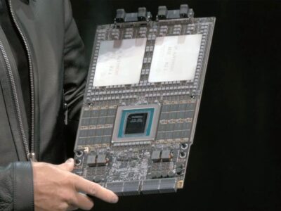
Synopsys has taped out a test chip using TSMC’s CoWoS interposer technology with full support for test, monitor, debug, and repair capabilities. The diagnosis, traceability, and mission mode signal integrity monitoring allow in-design, in-ramp, in-production, and in-field optimization for purposes such as predictive maintenance. The Monitoring, Test, and Repair (MTR) IP for UCIe PHY provides testability at the die, die-to-die interface and multi-die package levels.
Synopsys has achieved multiple silicon successes for UCIe and HBM3 IP solutions across N3E and N5 process technologies, accelerating IP integration and minimizing risk. Latest developments of the Synopsys UCIe IP, operating up to 40G, allows maximum bandwidth and energy efficiency without the need for additional area while the HBM4 and 3DIO IP solutions accelerate heterogeneous integration of 3D stacked-dies on TSMC’s advanced processes.
Synopsys is currently in the process of acquiring Ansys.
www.synopsys.com; www.tsmc.com; www.ansys.com
 If you enjoyed this article, you will like the following ones: don't miss them by subscribing to :